In today’s era of high-performance electronics, where devices are smaller, faster, and more powerful than ever before, multilayer PCB assembly stands as a cornerstone of advanced circuit design and manufacturing. From smartphones and medical equipment to aerospace controls and data servers, multilayer PCBs form the foundation of reliable and complex electronic systems. Understanding how these intricate boards are designed, manufactured, and assembled is essential for anyone involved in modern electronics production.
What Is Multilayer PCB Assembly?
Multilayer PCB assembly refers to the process of fabricating and assembling printed circuit boards that consist of more than two conductive layers. Unlike single- or double-sided PCBs, multilayer boards include multiple copper layers separated by insulating materials and laminated together to form a compact and high-density structure.
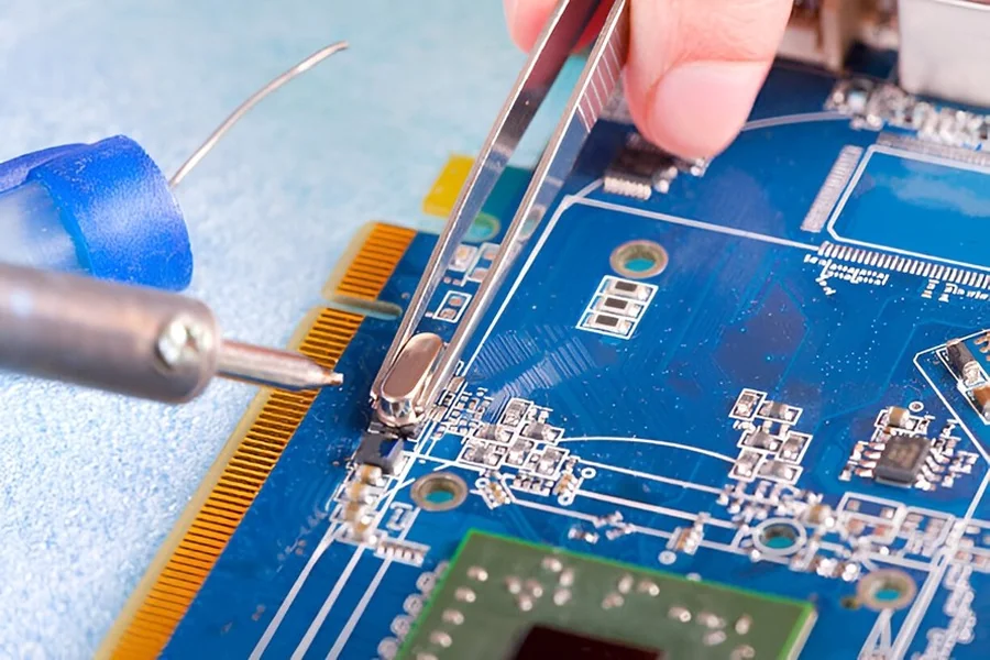
The assembly process involves mounting electronic components—both surface-mount (SMT) and through-hole—onto the top and bottom layers, while inner layers serve as signal, ground, or power planes. This configuration allows for more complex routing, reduced interference, and enhanced electrical performance.
Structure and Design of a Multilayer PCB
The structure of a multilayer PCB assembly is carefully engineered to achieve compactness without compromising performance. These boards are composed of alternating layers of conductive copper and dielectric insulation. Common configurations include 4-layer, 6-layer, 8-layer, and even 20-layer boards for high-end applications.
A typical stack-up includes:
- Core Layers: Pre-preg and copper sheets laminated together to form the inner structure.
- Signal Layers: Dedicated paths for data transmission and communication.
- Ground and Power Planes: Provide stable reference voltages and reduce electromagnetic interference (EMI).
- Top and Bottom Layers: Contain surface-mounted components and connectors for external connections.
Proper design ensures minimal signal loss, optimal impedance control, and mechanical stability—making the PCB suitable for high-frequency and high-speed applications.
The Importance of Multilayer PCB Assembly in Modern Electronics
The transition from single and double-sided boards to multilayer PCB assembly has been a major leap in electronics manufacturing. The main advantages include:
-
Contents
Compact Design with High Functionality
As devices become smaller and more powerful, multilayer PCBs provide the necessary density to accommodate complex circuits within minimal space. This is essential for smartphones, laptops, and wearable technology.
-
Enhanced Electrical Performance
Multiple layers allow designers to separate signal and ground planes, which helps minimise noise, cross-talk, and signal interference. This results in better signal integrity and higher operational efficiency.
-
Increased Durability and Strength
Multilayer boards are built using heat-resistant and durable materials that can withstand thermal and mechanical stress, ensuring long product life even under demanding conditions.
-
Improved Design Flexibility
Engineers can create sophisticated layouts and multi-functional systems on a single board, enabling innovative product designs without adding excessive bulk.
The Process of Multilayer PCB Assembly
The multilayer PCB assembly process involves several critical stages, each requiring precision and expertise to ensure quality and performance.
-
PCB Fabrication
The manufacturing process begins with designing the multilayer layout using CAD software. Each layer is etched, laminated, and pressed under controlled heat and pressure to form a compact and stable board.
-
Component Placement
Automated pick-and-place machines accurately position components on the board surface. Depending on the design, components may be placed on one or both sides.
-
Soldering
Surface mount components are soldered using reflow soldering, while through-hole parts may be attached using wave soldering or selective soldering. This creates strong and reliable electrical connections.
-
Inspection and Testing
After soldering, each board undergoes automated optical inspection (AOI), X-ray analysis, and functional testing to detect any soldering defects, shorts, or misalignments. Testing ensures that the assembled boards perform as designed.
-
Cleaning and Finishing
Flux residues are cleaned off, and the board is given protective coatings or surface finishes like ENIG (Electroless Nickel Immersion Gold) or HASL (Hot Air Solder Leveling) to enhance durability and solderability.
Applications of Multilayer PCB Assembly
Multilayer PCB assembly is essential in industries that demand high reliability and superior electrical performance, such as:
- Telecommunications: Routers, switches, and signal processors rely on multilayer PCBs for high-speed data transmission.
- Medical Equipment: Diagnostic machines, imaging systems, and monitoring devices require stable, noise-free operation.
- Automotive Electronics: Advanced Driver Assistance Systems (ADAS), sensors, and infotainment systems use multilayer PCBs for efficiency and safety.
- Aerospace and Defence: Aircraft navigation, control systems, and radar equipment depend on multilayer assemblies that can endure extreme conditions.
- Consumer Electronics: Smartphones, tablets, and gaming consoles rely on multilayer technology for compact design and performance.
Challenges in Multilayer PCB Assembly
While multilayer PCBs offer unmatched performance, their assembly presents specific challenges:
- Thermal Management: With higher component density, managing heat dissipation becomes crucial.
- Signal Integrity: Ensuring minimal signal loss across multiple layers requires precise impedance control.
- Manufacturing Complexity: The lamination and drilling of multiple layers demand accuracy to avoid alignment errors and internal shorts.
- Cost Considerations: The materials, processes, and testing involved in multilayer boards make them more expensive than simpler alternatives.
Overcoming these challenges requires advanced machinery, skilled engineers, and strict quality control protocols.
The Future of Multilayer PCB Assembly
As electronic devices continue to evolve, multilayer PCB assembly will become even more integral. Innovations in materials such as high-frequency laminates, flexible substrates, and embedded components are pushing the limits of what multilayer PCBs can achieve. Additionally, as demand for compact yet powerful electronics grows, more manufacturers are investing in automation and AI-driven inspection systems to ensure higher yields and precision.
Conclusion
Multilayer PCB assembly has revolutionised electronic manufacturing by enabling complex, compact, and high-speed devices to function efficiently. Its unmatched reliability, electrical performance, and design versatility make it indispensable across industries.
To ensure the highest quality and precision in your electronics, partnering with experienced providers of printed circuit board assembly services is essential. They offer advanced capabilities, state-of-the-art equipment, and expert engineering support to bring your complex designs to life—delivering consistent, high-performance PCBs that drive innovation forward.

